1920 × 1080
12.8-inch TFT LCD with a 283.39 × 159.41 mm active area.

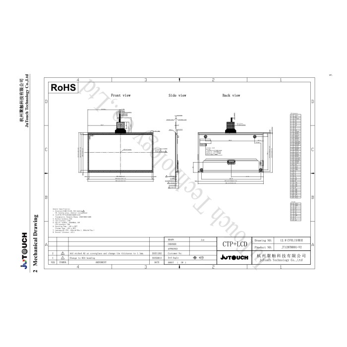
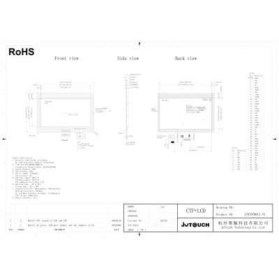
JT128TM001-V2 is a 12.8-inch CTP + LCD module with 1920 × 1080 resolution, LVDS video and USB / I2C touch interfaces. It combines a G+G touch structure with optical bonding, an ILI2511 controller, 10 touch points and an etched anti-glare surface.
This page is based on the preliminary specification dated January 12, 2026. Optical-table luminance is 560 nits typical with CTP. The mechanical drawing separately lists 800 nits; this discrepancy requires confirmation before design approval. No 800-nit or sunlight-readable claim is made here.
12.8-inch TFT LCD with a 283.39 × 159.41 mm active area.
G+G+LCD structure, etched AG surface and 6H hardness.
ILI2511 controller; USB / I2C touch interfaces.
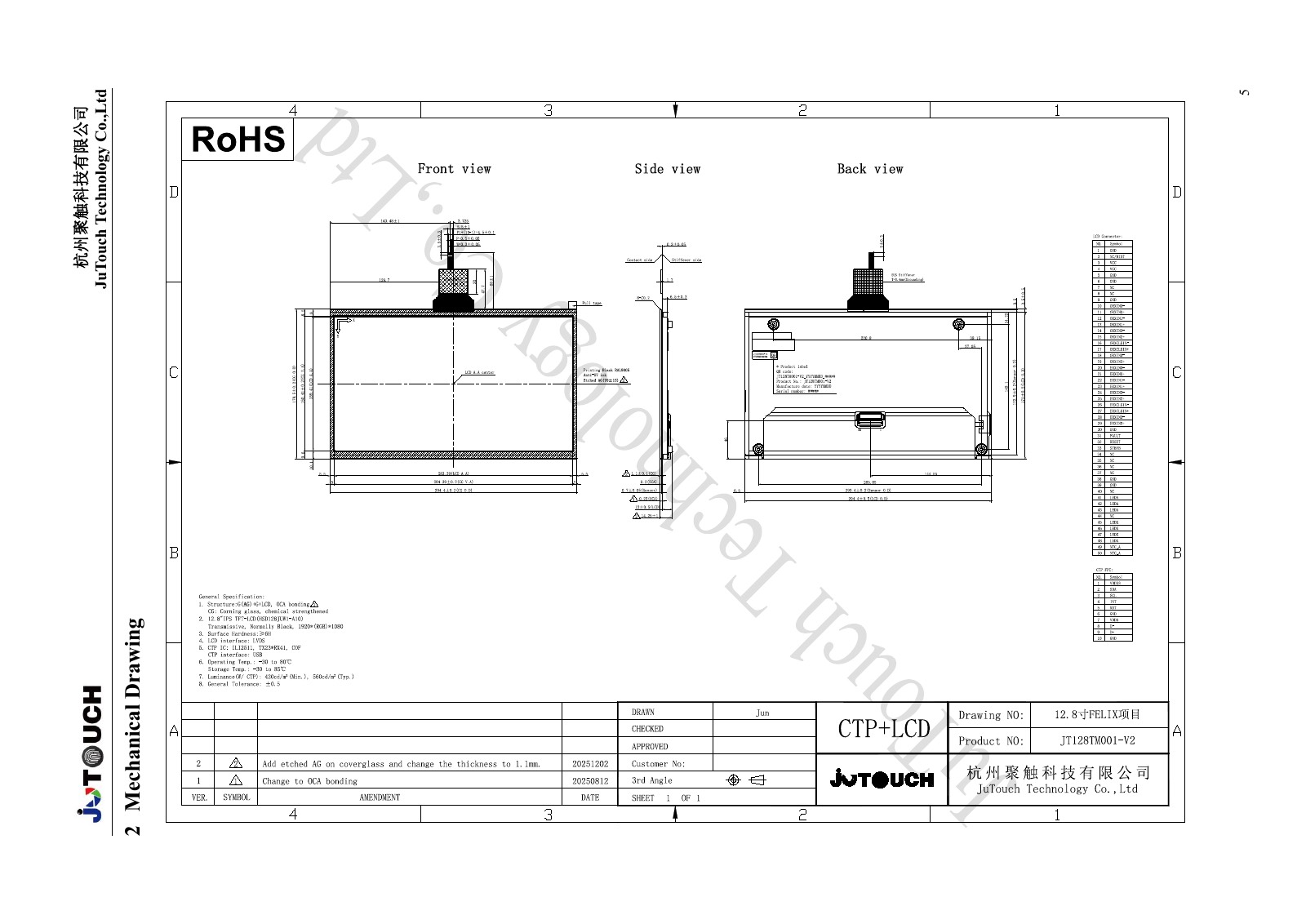
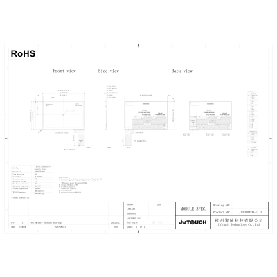
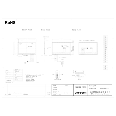
Outline dimensions: 294.4 × 178.5 × 14.25 mm, excluding PCBA. View the full-size drawing.
| Parameter | Specification |
|---|---|
| Module size | 12.8 inches |
| Structure | G+G+LCD; optical bonding |
| Resolution | 1920(RGB) × 1080 |
| Display mode | Normally black, transmissive |
| Pixel pitch | 0.1476(W) × 0.1476(H) mm |
| Pixel arrangement | RGB stripe |
| Viewing direction | ALL O’clock |
| Outline | 294.4(W) × 178.5(H) × 14.25(D) mm; W/O PCBA |
| Active area | 283.39(W) × 159.41(H) mm |
| LCD interface | LVDS |
| CTP interface | USB / I2C |
| CTP controller | ILI2511 |
| Touch points | 10 |
| Surface hardness | 6H |
| Surface treatment | Etched AG |
50-pin FPC connector: AORORA F31L-1A7H1-21050 or BJD 101049-205050, as named in the source. NTC: Murata NCU15XH103F6SRC.
| Pin | Symbol | Description |
|---|---|---|
| 1 | GND | Power ground |
| 2 | NC/BIST | No connector (BIST pin) |
| 3 | VCC | Digital power / Vin = 3.3 V |
| 4 | VCC | Digital power / Vin = 3.3 V |
| 5 | GND | Power ground |
| 6 | GND | Power ground |
| 7 | NC | No connector |
| 8 | NC | No connector |
| 9 | GND | Power ground |
| 10 | ORXIN0- | LVDS differential input: Negative odd data 0 |
| 11 | ORXIN0+ | LVDS differential input: Positive odd data 0 |
| 12 | ORXIN1- | LVDS differential input: Negative odd data 1 |
| 13 | ORXIN1+ | LVDS differential input: Positive odd data 1 |
| 14 | ORXIN2- | LVDS differential input: Negative odd data 2 |
| 15 | ORXIN2+ | LVDS differential input: Positive odd data 2 |
| 16 | ORXCLKIN- | LVDS differential input: Negative odd clock |
| 17 | ORXCLKIN+ | LVDS differential input: Positive odd clock |
| 18 | ORXIN3- | LVDS differential input: Negative odd data 3 |
| 19 | ORXIN3+ | LVDS differential input: Positive odd data 3 |
| 20 | ERXIN0- | LVDS differential input: Negative even data 0 |
| 21 | ERXIN0+ | LVDS differential input: Positive even data 0 |
| 22 | ERXIN1- | LVDS differential input: Negative even data 1 |
| 23 | ERXIN1+ | LVDS differential input: Positive even data 1 |
| 24 | ERXIN2- | LVDS differential input: Negative even data 2 |
| 25 | ERXIN2+ | LVDS differential input: Positive even data 2 |
| 26 | ERXCLKIN- | LVDS differential input: Negative even clock |
| 27 | ERXCLKIN+ | LVDS differential input: Positive even clock |
| 28 | ERXIN3- | LVDS differential input: Negative even data 3 |
| 29 | ERXIN3+ | LVDS differential input: Positive even data 3 |
| 30 | GND | Power ground |
| 31 | FAULT | Normal = L; abnormal = H |
| 32 | RESET | Global reset, active low |
| 33 | STBYB | Standby mode, active low |
| 34 | NC | No connector (serial chip enable CSB) |
| 35 | NC | No connector (serial clock SCL) |
| 36 | NC | No connector (serial data CDA) |
| 37 | NC | No connector (serial data CDA) |
| 38 | GND | Power ground |
| 39 | GND | Power ground |
| 40 | NC | No connector |
| 41 | LEDA | LED power (anode) |
| 42 | LEDA | LED power (anode) |
| 43 | LEDA | LED power (anode) |
| 44 | NC | No connector |
| 45 | LEDK | Cathode 1 |
| 46 | LEDK | Cathode 2 |
| 47 | LEDK | Cathode 3 |
| 48 | LEDK | Cathode 4 |
| 49 | NTC_A | NTC anode |
| 50 | NTC_K | NTC cathode |
| Pin | Symbol | Description |
|---|---|---|
| 1 | VDD33 | I2C power supply: 3.3 V |
| 2 | SDA | I2C data |
| 3 | SCL | I2C clock |
| 4 | INT | I2C interrupt |
| 5 | RST | Reset, active low |
| 6 | GND | Power ground |
| 7 | VDD5 | USB power supply: 5 V |
| 8 | D- | USB data minus |
| 9 | D+ | USB data plus |
| 10 | GND | Power ground |
These are source-listed limits, not nominal supply settings.
| Parameter | Symbol | Min. | Max. | Unit |
|---|---|---|---|---|
| Power supply | VCC | -0.3 | 4 | V |
| Operating temperature | TOP | -30 | +85 | °C |
| Storage temperature | TST | -40 | +90 | °C |
| Item | Symbol | Min. | Typ. | Max. | Unit | Condition |
|---|---|---|---|---|---|---|
| Supply voltage | VCC | 3 | 3.3 | 3.6 | V | — |
| Input high | ViH | VCC × 0.7 | — | VCC | V | — |
| Input low | ViL | 0 | — | VCC × 0.3 | V | — |
| Supply current | IDD | — | — | 500 | mA | VCC=3.3 V, white pattern |
| Inrush current | IRUSH | — | — | 2.0 | A | Source test circuit; 2 ms rising time |
| Item | Symbol | Min. | Typ. | Max. | Unit | Condition |
|---|---|---|---|---|---|---|
| Differential high threshold | Vth | — | — | 100 | mV | VCM=1.2 V |
| Differential low threshold | Vtl | -100 | — | — | mV | VCM=1.2 V |
| Input current | IIN | -10 | — | +10 | µA | — |
| Differential input voltage | |VID| | 0.1 | — | 0.6 | V | — |
| Common-mode voltage offset | VCM | 1 | 1.2 | 1.7 − (|VID| / 2) | V | — |
| Item | Symbol | Min. | Typ. | Max. | Unit |
|---|---|---|---|---|---|
| Frame rate | FR | 55 | 60 | 65 | Hz |
| Vertical display time | Tvd | — | 1080 | — | H |
| Vertical pulse width | Tvpw | 1 | 3 | 20 | H |
| Vertical back porch | Tvbp | 2 | 24 | 200 | H |
| Vertical front porch | Tvfp | 5 | 8 | 200 | H |
| Frame period | Tv | 1087 | 1112 | 1404 | H |
| Horizontal display time | Thd | — | 960 | — | DCLK |
| Horizontal pulse width | Thpw | 10 | 12 | 200 | DCLK |
| Horizontal back porch | Thbp | 5 | 16 | 200 | DCLK |
| Horizontal front porch | Thfp | 24 | 26 | 200 | DCLK |
| One horizontal line | Tv (source label) | 989 | 1012 | 1248 | DCLK |
| Clock rate | FDCLK | 64.5 | 66.9 | 80 | MHz |
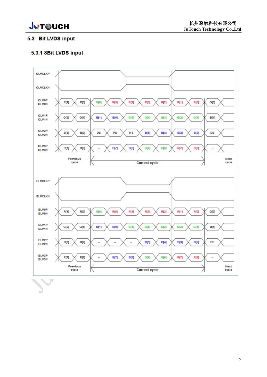
The horizontal-display timing is for two-port LVDS; it does not change the 1920 × 1080 panel resolution.
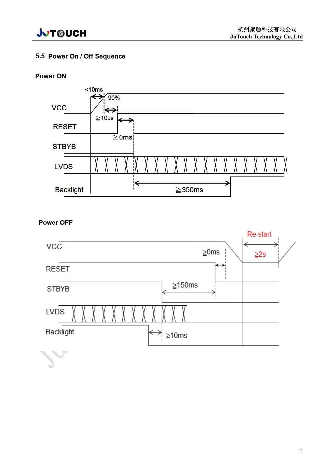
Follow the source sequence for VCC, RESET, STBYB, LVDS and backlight. The diagram lists a restart interval of at least 2 seconds.
| Parameter | Symbol | Min. | Typ. | Max. | Unit | Source condition |
|---|---|---|---|---|---|---|
| LED current | IF | — | 340 | — | mA | Ta=25°C |
| LED voltage | VF | — | 38.4 | 40.8 | V | Ta=25°C |
The source lifetime table and its notes use different current conditions. No lifetime claim is made until these are reconciled. The source specifies a 12S4P, 48-LED circuit and recommends constant-current drive. Review the full backlight thermal/current requirements before integration.
| Item | Condition | Min. | Typ. | Max. | Unit |
|---|---|---|---|---|---|
| Viewing angle: Horizontal θx+ | CR ≥ 10 | 80 | 85 | — | degrees |
| Viewing angle: Horizontal θx- | CR ≥ 10 | 80 | 85 | — | degrees |
| Viewing angle: Vertical θy+ | CR ≥ 10 | 80 | 85 | — | degrees |
| Viewing angle: Vertical θy- | CR ≥ 10 | 80 | 85 | — | degrees |
| Luminance with CTP | θx=0°, θy=0° | 420 | 560 | — | nit |
| 9-point uniformity | θx=0°, θy=0° | 70 | 80 | — | % |
| Contrast ratio | θx=0°, θy=0° | — | 1400 | — | — |
| Response time TR+TF | — | — | 25 | 30 | ms |
| CIE 1931 Wx | θx=0°, θy=0°; R=G=B=255; gray scale | Typ. − 0.05 | TBD | Typ. + 0.05 | — |
| CIE 1931 Wy | θx=0°, θy=0°; R=G=B=255; gray scale | Typ. − 0.05 | TBD | Typ. + 0.05 | — |
| CIE 1931 Rx | θx=0°, θy=0°; R=G=B=255; gray scale | Typ. − 0.05 | TBD | Typ. + 0.05 | — |
| CIE 1931 Ry | θx=0°, θy=0°; R=G=B=255; gray scale | Typ. − 0.05 | TBD | Typ. + 0.05 | — |
| CIE 1931 Gx | θx=0°, θy=0°; R=G=B=255; gray scale | Typ. − 0.05 | TBD | Typ. + 0.05 | — |
| CIE 1931 Gy | θx=0°, θy=0°; R=G=B=255; gray scale | Typ. − 0.05 | TBD | Typ. + 0.05 | — |
| CIE 1931 Bx | θx=0°, θy=0°; R=G=B=255; gray scale | Typ. − 0.05 | TBD | Typ. + 0.05 | — |
| CIE 1931 By | θx=0°, θy=0°; R=G=B=255; gray scale | Typ. − 0.05 | TBD | Typ. + 0.05 | — |
“—” means not specified; TBD values remain unresolved. Source measurement guidance specifies 30-minute stabilization and 30-minute backlight warm-up in a windless room. White uniformity is minimum divided by maximum luminance across nine points, multiplied by 100%.
These are specification test conditions, not independent certification or proof of completed qualification.
| Test | Condition |
|---|---|
| High-temperature storage | 90°C, 240 hours |
| Low-temperature storage | -40°C, 240 hours |
| High-temperature operation | 85°C, 240 hours |
| Low-temperature operation | -30°C, 240 hours |
| High temperature / high humidity operation | 60°C, 90% RH, 240 hours |
| Thermal shock, non-operation | -30°C/30 min to +85°C/30 min; 5-min change; 100 cycles |
| ESD | Contact ±8 kV; air ±15 kV; R=330 Ω, C=150 pF |
The source requires no surface condensation during testing, a maximum display-surface temperature of 85°C and at least 24 hours of recovery at room temperature before cosmetic/function inspection.
Confirm the preliminary specification revision, brightness discrepancy, backlight current/lifetime conditions, mechanical fit and host LVDS compatibility before sample approval. Supply the model number, required quantity, host details and enclosure drawing when making an inquiry.
Contact JuTouch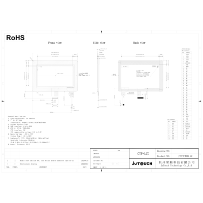

+86 0571-86222850